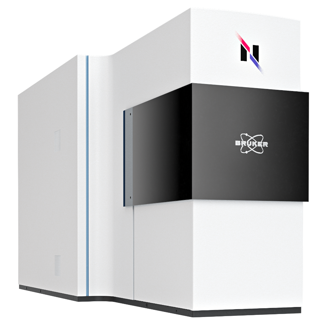
Bruker Nanophoton Series Microscopes

Nanophoton Raman Microscopes
Nanophoton Raman microscopes combine high-resolution Raman spectroscopy with advanced galvanometer scanning technology for fast and precise chemical imaging. Designed for research and industrial applications, these systems enable detailed analysis of materials at the microscopic scale, with high speed, sensitivity, and spatial resolution.
The Nanophoton RAMANfamily includes versatile solutions for point analysis, high-speed Raman imaging, and large-area or wafer analysis, making the systems suitable for a wide range of applications in materials science, pharmaceuticals, electronics, batteries, polymers, and life sciences.
RAMANtouch
RAMANwalk
RAMANdrive
VIDEO
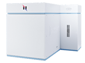
RAMANtouch Confocal Raman Microscope
The RAMANtouch is a high-performance confocal Raman microscope designed for fast and precise chemical imaging. It combines advanced laser scanning technology with high spectral and spatial resolution, enabling detailed analysis of materials and samples in both 2D and 3D.
Key advantages:
- High-speed Raman imaging for rapid sample analysis
- Excellent spectral and spatial resolution
- 2D and 3D Raman imaging capabilities
- Confocal optical system for precise depth analysis
- Automated calibration and optical alignment
- Laser scanning without moving the sample stage
- Non-destructive analysis of materials and structures
The RAMANtouch is suitable for a wide range of research and industrial applications, including materials science, semiconductors, batteries, pharmaceuticals, polymers, minerals, and life sciences. Its combination of speed, precision, and automation makes it an effective solution for both routine analysis and advanced Raman imaging.
For more information, please visit the manufacturer’s website
RAMANwalk Confocal Raman Microscope
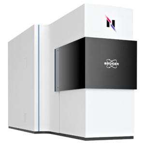
The RAMANwalk is an advanced confocal Raman microscope designed for fast and efficient Raman imaging. Its innovative random-walk scanning technology intelligently searches for Raman signals, enabling rapid image previews and significantly reducing measurement time compared with conventional scanning methods.
Key advantages:
- Innovative random-walk technology for faster Raman imaging
- Rapid Raman image previews for quick sample evaluation
- High spectral and spatial resolution
- Galvanic mirrors for fast and precise laser beam steering
- Automated hardware, calibration, and optical alignment
- Powerful 2D and 3D Raman imaging capabilities
- Efficient identification of specific chemical components and regions of interest
The RAMANwalk is particularly well suited for routine Raman analysis and applications where rapid identification or screening of sample components is required. It can be used in battery research, semiconductors, pharmaceuticals, life sciences, polymers, minerals, food, and other materials research.
For more information, please visit the manufacturer’s website
RAMANdrive Wafer Analysis System
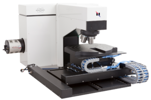
The RAMANdrive is a specialized Raman microscope designed for ultra-fast, high-resolution wafer analysis, particularly for semiconductor research and development. It features a dedicated 300 mm motorized wafer stage, providing excellent stability, precision, and access across the entire wafer surface.
Key advantages:
- Ultra-fast Raman imaging with high spectral and spatial resolution
- Dedicated 300 mm wafer stage for large-area analysis
- Precise Stage Navigation System for automated positioning of areas of interest
- Up to 400 spectra captured in a single laser shot
- AreaFlash™ technology for rapid large-area Raman imaging
- Detection and identification of particles smaller than 100 nm
- 3D Raman imaging for stress and polytype distribution analysis
- Automated wavenumber calibration and optical alignment
RAMANdrive is ideally suited for semiconductor and advanced materials research, including wafer inspection, particle analysis, stress evaluation, polytype characterization, defect analysis, and photoluminescence imaging.
For more information, please visit the manufacturer’s website
Product Related
Bruker SENTERRA II
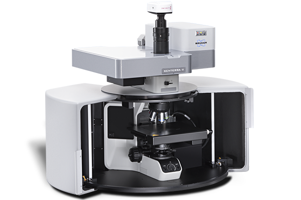
Bruker SENTERRA II – Confocal Raman Microscope Bruker SENTERRA II is a compact and fully automated confocal Raman microscope designed…
Bruker Nanophoton Series Microscopes
Nanophoton Raman Microscopes Nanophoton Raman microscopes combine high-resolution Raman spectroscopy with advanced galvanometer scanning technology for fast and precise chemical…